This article illustrates some typical applications of operational amplifiers. A simplified schematic notation is used, and the reader is reminded that many details such as device selection and power supply connections are not shown.
Linear circuit applications
Comparator:

Comparator
Compares two voltages and switches its output to indicate which voltage is larger.

(where Vs is the supply voltage and the opamp is powered by + Vs and − Vs.)
Inverting amplifier:
An inverting amplifier uses negative feedback to invert and amplify a voltage. The Rf resistor allows some of the output signal to be returned to the input. Since the output is 180° out of phase, this amount is effectively subtracted from the input, thereby reducing the input into the operational amplifier. This reduces the overall gain of the amplifier and is dubbed negative feedback.

-
-
A third resistor, of value , added between the non-inverting input and ground, while not necessary, minimizes errors due to input bias currents.
The gain of the amplifier is determined by the ratio of Rf to Rin. That is:

The presence of the negative sign is a convention indicating that the output is inverted. For example, if Rf is 10,000 Ω and Rin is 1,000 Ω, then the gain would be -10000Ω/1000Ω, which is -10.
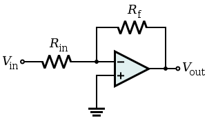
Non-inverting amplifier:

Amplifies a voltage (multiplies by a constant greater than 1)
-
Input impedance
-
The input impedance is at least the impedance between non-inverting ( + ) and inverting ( − ) inputs, which is typically 1 MΩ to 10 TΩ, plus the impedance of the path from the inverting ( − ) input to ground (i.e., R1 in parallel with R2). -
Because negative feedback ensures that the non-inverting and inverting inputs match, the input impedance is actually much higher. -
- A resistor of value
- which is the equivalent resistance of R1 in parallel with R2, between the Vin source and the non-inverting ( + ) input will ensure the impedances looking out of each input will be matched.
-

Differential amplifier:

The circuit shown is used for finding the difference of two voltages each multiplied by some constant (determined by the resistors).
The name "differential amplifier" should not be confused with the "differentiator", also shown on this page.

-
Differential Zin (between the two input pins) = R1 + R2 (Note: this is approximate) Differential amplifier
Voltage follower:

Voltage follower
Used as a buffer amplifier to eliminate loading effects (e.g., connecting a device with a high source impedance to a device with a low input impedance).

 (realistically, the differential input impedance of the op-amp itself, 1 MΩ to 1 TΩ)
Due to the strong (i.e., unity gain) feedback and certain non-ideal characteristics of real operational amplifiers, this feedback system is prone to have poor stability margins. Consequently, the system may be unstable when connected to sufficiently capacitive loads. In these cases, a lag compensation network (e.g., connecting the load to the voltage follower through a resistor) can be used to restore stability. The manufacturer data sheet for the operational amplifier may provide guidance for the selection of components in external compensation networks. Alternatively, another operational amplifier can be chosen that has more appropriate internal compensation.
Summing amplifier:

A summing amplifer sums several (weighted) voltages:

-
When , and Rf independent

-
When

-
Output is inverted -
Integrator:

Integrates the (inverted) signal over time

(where Vin and Vout are functions of time, Vinitial is the output voltage of the integrator at time t = 0.)
-
Note that this can also be viewed as a low-pass electronic filter. It is a filter with a single pole at DC (i.e., where ω = 0) and gain. -
There are several potential problems with this circuit.-
It is usually assumed that the input Vin has zero DC component (i.e., has a zero average value). Otherwise, unless the capacitor is periodically discharged, the output will drift outside of the operational amplifier's operating range. -
Even when Vin has no offset, the leakage or bias currents into the operational amplifier inputs can add an unexpected offset voltage to Vin that causes the output to drift. Balancing input currents and replacing the non-inverting ( + ) short-circuit to ground with a resistor with resistance R can reduce the severity of this problem. -
Because this circuit provides no DC feedback (i.e., the capacitor appears like an open circuit to signals with ω = 0), the offset of the output may not agree with expectations (i.e., Vinitial may be out of the designer's control with the present circuit).
-
- Many of these problems can be made less severe by adding a large resistor RF in parallel with the feedback capacitor. At significantly high frequencies, this resistor will have negligible effect. However, at low frequencies where there are drift and offset problems, the resistor provides the necessary feedback to hold the output steady at the correct value. In effect, this resistor reduces the DC gain of the "integrator" – it goes from infinite to some finite value RF / R.
Differentiator:

Differentiates the (inverted) signal over time.
- The name "differentiator" should not be confused with the "differential amplifier," which is also shown on this page. The former takes a derivative and the latter takes a difference (i.e., does subtraction). This is a circuit that could be used in an analog computer, but in practice these circuits are difficult to keep stable and noise-free, so often the problem can be rearranged to use an integrator instead.

-
Note that this can also be viewed as a high-pass electronic filter. It is a filter with a single zero at DC (i.e., where ω = 0) and gain.
Instrumentation amplifier:

Combines very high input impedance, high common-mode rejection, low DC offset, and other properties used in making very accurate, low-noise measurements
-
Is made by adding a non-inverting buffer to each input of the differential amplifier to increase the input impedance.
Schmitt trigger:

Schmitt trigger with non-inverting hysteretic switching characteristic
In this configuration, the hysteresis curve is non-inverting (i.e., very negative inputs correspond to a negative output and very positive inputs correspond to a positive output), and the switching thresholds are  where Vsat is the greatest output magnitude of the operational amplifier.
where Vsat is the greatest output magnitude of the operational amplifier.
Schmitt trigger with inverting hysteretic switching characteristic
Alternatively, the input and the ground may be swapped. In this configuration, the hysteresis curve is inverting (i.e., very negative inputs correspond to a positive output and vice versa), and the switching thresholds are  . Such a configuration is used in the relaxation oscillator shown below.
. Such a configuration is used in the relaxation oscillator shown below.Relaxation oscillator:

Relaxation oscillator implemented with inverting Schmitt trigger and RC network
By using an RC network to add slow negative feedback to the inverting Schmitt trigger, a relaxation oscillator is formed. The feedback through the RC network causes the Schmitt trigger output to oscillate in an endless symmetric square wave (i.e., the Schmitt trigger in this configuration is an astable multivibrator).
Inductance gyrator:

DAHIANA ALEJANDRA ROSALES HERNÁNDEZ
EES
Invite your mail contacts to join your friends list with Windows Live Spaces. It's easy! Try it!
No hay comentarios:
Publicar un comentario